Huang's Law Beyond Moore's Law — The Feynman Architecture Ushers in the Age of Light
NVIDIA unveiled the Feynman architecture at GTC 2026, slated for 2028. Leveraging silicon photonics to replace copper with light, promising 14x performance over Blackwell, Feynman declares the end of the fundamental power and bandwidth bottlenecks that have constrained AI infrastructure.
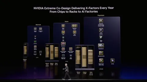
Jensen Huang always flips one more slide on stage. GTC 2026 was no exception. Blackwell Ultra shipping, Vera Rubin mass production confirmed, and then one name on the final slide: Feynman. The industry calls it Huang's Law — at every GTC, Huang unveils architectures that more than double the performance of their predecessors, outpacing the 18-to-24-month doubling cycle of Moore's Law. Feynman, arriving in 2028, may be the most dramatic chapter of that law yet. It is a declaration that data will travel on light, not electricity. An acknowledgment of copper wiring's physical limits and a leap to optical interconnects. In semiconductor history, changing the transmission medium itself is a rare event.
From Blackwell to Feynman: Milestones Every Two Years

"We deliver new AI infrastructure on a one-year cadence. Huang's Law — faster than Moore's Law." — Jensen Huang, GTC 2026
NVIDIA's GPU roadmap now runs like clockwork. Blackwell dominates current data centers; Vera Rubin enters mass production from late 2026 through 2027; Feynman arrives in 2028. Each architecture borrows its name from giants of physics and astronomy. Richard Feynman was the father of quantum electrodynamics and a Nobel laureate. The name alone reveals the weight NVIDIA places on this architecture.
| Architecture | Process | Timeline | Key Feature |
|---|---|---|---|
| Blackwell | TSMC 3nm | 2024–present | Current-gen AI training/inference standard |
| Vera Rubin | Next-gen process | Late 2026–2027 | HBM4 integration, next-gen NVLink |
| Feynman | TSMC A16 | 2028 | Silicon photonics, 14x over Blackwell |
The Moment Light Replaces Copper

The core of Feynman is silicon photonics. Today, data transfer between chips, boards, and racks relies entirely on electrical signals through copper wiring. The problem is that copper has hit its physical limits. Increasing bandwidth means adding more wires, and more wires mean exploding heat and power consumption. As AI models grow exponentially, a paradox has emerged: the energy spent moving data exceeds the energy spent computing.
Silicon photonics uses optical signals instead of electrical ones. Light offers overwhelmingly greater bandwidth than copper, suffers minimal loss over distance, and generates virtually no heat. NVIDIA embedding silicon photonics in Feynman means fundamentally redesigning interconnects inside data centers. It is the first attempt to apply optical interconnects to a commercial AI chip.
Copper wiring's limits are no longer an engineering problem — they are a physical wall. Silicon photonics does not bypass that wall; it removes it entirely.
TSMC A16 and the Dawn of the Angstrom Era

Feynman will be fabricated on TSMC's A16 process — a leap from Blackwell's 3-nanometer process to angstrom scale. One angstrom equals 0.1 nanometers, meaning transistor sizes approach the scale of a few atoms. TSMC A16 applies backside power delivery technology to push transistor density to its limits while maintaining power efficiency.
The nanometer-to-angstrom transition is more than a number change. As process shrinks approach physical limits, traditional methods can no longer improve performance. TSMC A16 tackles this challenge with a new structure that delivers power from the backside while making transistors smaller. This is the physical foundation that allows Feynman to promise 14x performance over Blackwell.
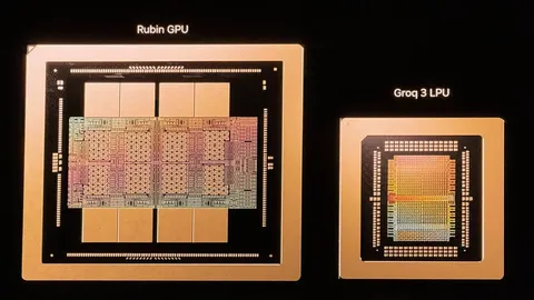
The Secret to 14x Performance Is Not a Single Chip
The 14x figure over Blackwell is not a chip-to-chip comparison. NVIDIA is redesigning the entire system for the Feynman generation. A new GPU integrates with the LPU (LP40), CPU (Rosa), and network chip (BlueField-5), bound together by the Kyber rack architecture. Kyber achieves both scale-up and scale-out through a copper/CPO (Co-Packaged Optics) hybrid approach.
| Component | Role | Generational Change |
|---|---|---|
| GPU (Feynman) | Core AI compute | Silicon photonics + A16 process |
| LPU (LP40) | Low-power inference acceleration | Evolved inference-dedicated processor |
| CPU (Rosa) | Host processor | GPU-CPU integration optimized |
| BlueField-5 | Data Processing Unit (DPU) | Enhanced network offload |
| Kyber Rack | System architecture | Copper/CPO hybrid interconnect |
The key is not single-chip performance but the connections between chips. No matter how fast a GPU gets, system performance stalls if data transfer is the bottleneck. This is why Feynman introduces silicon photonics and the Kyber architecture simultaneously — computational and transfer performance must rise together for 14x to become reality.
The Invisible Wall Called Power
The biggest bottleneck for scaling AI infrastructure is not GPU count — it is power. Training a single large language model consumes as much electricity as a small city. Models keep growing, and the rise of agentic AI is causing inference demand to explode. Data center operators have already entered a war for power procurement.
Feynman's silicon photonics strikes at the heart of this power problem. Optical interconnects dramatically reduce energy consumption for data transfer compared to copper — moving the same data with less power and less heat. It breaks through the Power Wall at a physical level. If commercialized in 2028, the same power budget will handle far more AI computation, potentially transforming the cost structure of AI services.
Competitors' Clocks Don't Tick at the Same Speed
NVIDIA revealing its 2028 roadmap now is a message in itself. AMD is targeting AI accelerator market share expansion with its MI400 series, and Intel is attempting to enter the AI training market with its Gaudi series. But neither company has disclosed concrete 2028 roadmaps. NVIDIA's two-year advance roadmap is a clear signal to customers and investors.
The memory industry also needs to prepare. SK hynix and Samsung currently split the HBM (High Bandwidth Memory) market — a critical AI accelerator component — but the silicon photonics era fundamentally changes the interface between memory and processors. New memory technologies optimized for optical interconnects may be required. Feynman is a turning point that will send ripples through the entire memory supply chain, not just chip manufacturers.
What 2028 Will Change
If Feynman delivers on its promises, the economics of AI infrastructure will shift. Better power efficiency lowers data center operating costs, and those savings will be reflected in AI service pricing. New opportunities open for SMBs and startups currently priced out of large language model API calls. In an era where agentic AI runs thousands of agents simultaneously, lower cost and power barriers are not mere technical improvements — they are structural market changes.
Of course, a roadmap two years out carries uncertainty. Mass production of silicon photonics is unproven, and TSMC A16 yield is a variable. But NVIDIA disclosing a specific architecture name and technology stack on the GTC stage signals that internal design is well advanced. The age of copper is fading, and the age of light is coming. Whether Feynman becomes the first commercial chip of that transition — GTC 2028 will have the answer.